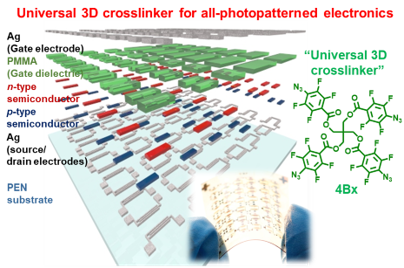
Universal Three-Dimensional Crosslinkers
for All-Photopatterned Electronics
Fabrication of electronic components at high resolution remains a challenging task for organic electronic devices fabricated entirely through a series of solution processes. We report all-solution processing of highly integrated arrays of polymer thin-film transistors (PTFTs) and logic gates. This processing is performed using a newly developed multi-bridged crosslinker containing four-branched photocrosslinkable units. Under UV, multi-bridged crosslinkers mixed within solution-processable electronic materials generate a three-dimensional (3D) network of the given material. We note that this multi-bridged crosslinker can produce the 3D network state efficiently even at an unprecedentedly small loading, which, in turn, enables preservation of the intrinsic electrical properties of the photocrosslinked material. Moreover, the crosslinking of electronic component layers allows not only micropatterning of the layers at high resolution but also stacking of a given electronic component layer on top of the other layers. Furthermore, we developed more efficient multi-bridged crosslinkers and used them for patterning various type of electronic polymers, quantum dots, and electrodes, and demonstrated high-performance electronic devices..

Related Publications
1. “Nondestructive Photopatterning of Heavy-Metal-Free Quantum Dots” Adv. Mater. 2022, 2205504.
2. “Low-Voltage Organic Transistors with Carrier Mobilities over 10 cm-1V-1s-1 Using Six-Branched Organic Azide” Chem. Mater. 2022, Published ASAP.
3. “Two-Color Strip-Patterned White OLEDs: Tunable Color-Temperature via Pattern Dimension Control” Adv. Opt. Mater. 2022, 2200456.
4. “Tetrabranched Photo-Crosslinker Enables Micrometer-Scale Patterning of Light-Emitting Super Yellow for High-Resolution OLEDs” ACS Photonics 2021, 8, 2519.
5. “Universal Three-Dimensional Crosslinker for All-Photopatterned Electronics” Nat. Commun. 2020, 11, 1520.
 2022 International Symposium on Chemical Applications of Mach...
 2022 International Symposium on Bioactive and Bioengineering ...