
Seo Eun Byeon(석사과정) / Miso Kim(석사과정)
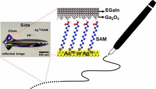
Since fabricating geometrically well-defined, noninvasive, and compliant electrical contacts over molecular monolayers is difficult, creating molecular-scale electronic devices that function in high yield with good reproducibility is challenging. Moreover, none of the previously reported methods to form organic–electrode contacts at the nanometer and micrometer scales have resulted in directly addressable contacts in an untethered form under ambient conditions without the use of cumbersome equipment and nanolithography. Here we show that in situ encapsulation of a liquid metal (eutectic Ga–In alloy) microelectrode, which is used for junction formation, with a convenient photocurable polymeric scaffold enables untethering of the electrode and direct writing of arbitrary arrays of high-yielding molecular junctions under ambient conditions in a maskless fashion. The formed junctions function in quantitative yields and can afford tunneling currents with high reproducibility; they also function at low temperatures and under bent. The results reported here promise a massively parallel printing technology to construct integrated circuits based on molecular junctions with soft top contacts.

http://pubs.acs.org/doi/abs/10.1021/acsami.7b14347
 Recent Progress in the Chemistry of Pyridazinones for Functio...
 Single Component Organic Solar Cells Based on Oligothiophene-...


